| NTE Type Number |
Description and Application |
Case Style |
Collector to Emitter Breakdown Voltage (Volts) |
Gate to Emitter Cutoff Voltage (Volts) |
Gate to Emitter Breakdown Voltage (Volts) |
Maximum Collector Current (Amps) |
Collector to Emitter Saturation Voltage (Volts) |
Input Capacitance (pf) |
Device Total Power Dissipation @ TC= +25°C (Watts) |
| V(BR)CES | VGE(Off) | BVGES | IC | VCE(sat) | Cies | PD | |||
|
3300 $12.68 |
N-CHANNEL Enhancement Mode High Speed Switch |
TO220 Full Pack |
400 Min | 7 Max | ±25 Max | 10 | 8.0 Max | 1350 Typ | 30 Max |
| tr = 0.50µs, ton = 0.50µs, tf = 6µs, toff = 7µs | |||||||||
|
3301 $11.90 |
N-CHANNEL Enhancement Mode High Speed Switch |
TO220 Full Pack |
400 Min | 7 Max | ±25 Max | 15 | 8.0 Max | 2000 Typ | 40 Max |
| tr = 0.50µs, ton = 0.50µs, tf = 6µs, toff = 7µs | |||||||||
|
3302 $8.79 |
N-CHANNEL Enhancement Mode High Speed Switch |
TO220 Full Pack |
600 Min | 6 Max | ±20 Max | 8 | 4.0 Max | 650 Typ | 30 Max |
| tr = 0.60µs, ton = 0.80µs, tf = 0.35µs, toff = 1µs | |||||||||
|
3303 $11.16 |
N-CHANNEL Enhancement Mode High Speed Switch |
TO220 Full Pack |
600 Min | 6 Max | ±20 Max | 15 | 4.0 Max | 1100 Typ | 35 Max |
| tr = 0.60µs, ton = 0.80µs, tf = 0.35µs, toff = 1µs | |||||||||
|
3310 $13.85 |
N-CHANNEL Enhancement Mode High Speed Switch |
TO3P | 600 Min | 6 Max | ±20 Max | 15 | 4.0 Max | 1100 Typ | 100 Max |
| tr = 0.60µs, ton = 0.80µs, tf = 0.35µs, toff = 1µs | |||||||||
|
3311 $19.36 |
N-CHANNEL Enhancement Mode High Speed Switch |
TO3P | 600 Min | 6 Max | ±20 Max | 25 | 4.0 Max | 1400 Typ | 150 Max |
| tr = 0.30µs, ton = 0.40µs, tf = 0.15µs, toff = 0.50µs | |||||||||
|
3320 $39.75 |
N-CHANNEL Enhancement Mode High Speed Switch |
- | 600 Min | 6 Max | ±20 Max | 50 | 2.0 Max | 7900 Typ | 240 Max |
| tr = 0.07µs, ton = 0.24µs, tf = 0.05µs, toff = 0.43µs | |||||||||
|
3322 $39.20 |
N-CHANNEL Enhancement Mode High Speed Switch |
- | 900 Min | 6 Max | ±25 Max | 60 | 3.7 Max | 5300 Typ | 200 Max |
| tr = 0.25µs, ton = 0.35µs, tf = 0.25µs, toff = 0.50µs | |||||||||
|
3323 $38.72 |
N-CHANNEL Enhancement Mode High Speed Switch |
- | 1200 Min | 6 Max | ±20 Max | 25 | 4.0 Max | 3200 Typ | 200 Max |
| tr = 0.30µs, ton = 0.40µs, tf = 0.25µs, toff = 0.80µs | |||||||||
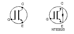
DESCRIPTION
NTE's series of Insulated Gate Bipolar Transistors (IGBTs) combine the high
input impedance and high speed characteristics of MOSFETs and the high
conduction (low saturation voltage) characteristics of bipolar transistors.
Their structure looks very much like a MOSFET except that MOSFETs use an N+ - N-
type substrate whereas IGBTs use a P+ - N- type substrate.
The thyristor fromed by PNP - NPN transistor coupling has its base and emitter shorted by aluminum patterning to disable it from operating and is therefore considered irrelevant to the basic operation of IGBTs. Consequently, the equivalent circuit and basic operating mechanism of IGBTs are the same as those of a MOS-input inverted Darlington transistor comprised of an N-channel enhancement MOSFET in its input stage and a PNP transistor on the output stage.
IGBTs are constructed in such a way that first, the gate voltage is applied to form a channel and then the base current of the PNP transistor is supplied, letting the circuit turn on eventually as an IGBT. Conversely, when turned off, the channel is eliminated to turn off the base current. Thus, IGBTs are driven in exactly the same way as MOSFETs, and IGBTs have high input impedance characteristics just like MOSFETs.